Issue 18, 2015

High performance H2 evolution realized in 20 μm-thin silicon nanostructured photocathodes

Abstract

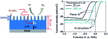
Thickness reduction in high-purity silicon wafers is beneficial for cost-efficient hydrogen evolution utilizing silicon photocathodes. However, two major issues need to be resolved: insufficient light absorption by a thin Si absorber and poor charge transfer reaction by dominant surface recombination. Here, we present 20 μm-thin Si photocathodes employing Pt-nanoparticle-coated silicon nanoholes that realize a photocurrent of 23 mA cm−2 (at 0 V vs. RHE) corresponding to the amount typically achieved by a conventional wafer (∼200 μm-thick).

Graphical abstract: High performance H2 evolution realized in 20 μm-thin silicon nanostructured photocathodes

Supplementary files

Article information

Article type
Communication
Submitted
08 Jan 2015
Accepted
01 Apr 2015
First published
02 Apr 2015

J. Mater. Chem. A, 2015,3, 9456-9460

Author version available

High performance H2 evolution realized in 20 μm-thin silicon nanostructured photocathodes

J. Jung, M. Park, X. Li, J. Kim, R. B. Wehrspohn and J. Lee, J. Mater. Chem. A, 2015, 3, 9456 DOI: 10.1039/C5TA00156K

To request permission to reproduce material from this article, please go to the Copyright Clearance Center request page.

If you are an author contributing to an RSC publication, you do not need to request permission provided correct acknowledgement is given.

If you are the author of this article, you do not need to request permission to reproduce figures and diagrams provided correct acknowledgement is given. If you want to reproduce the whole article in a third-party publication (excluding your thesis/dissertation for which permission is not required) please go to the Copyright Clearance Center request page.

Read more about how to correctly acknowledge RSC content.

Social activity

Spotlight

Advertisements