Layer-by-layer films for tunable and rewritable control of contact electrification†
Abstract
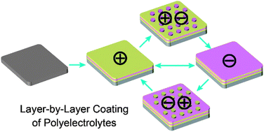
Charges generated by contact of solid surfaces (contact electrification) can be hazardous or useful depending on the circumstance. This paper describes a process to design a solid surface rationally to either induce or prevent charging during contact electrification; this process coats the surface with polyelectrolytes. It is observed experimentally that a surface coated with a layer of a polymer having multiple, covalently attached positive charges (a “polycation”) develops a positive charge after contacting another surface; a surface coated with a layer of polymer having negative charges (a “polyanion”) develops a negative charge. By coating the surface using layer-by-layer (LBL) deposition, the tendency of the surface to charge either positively or negatively can be switched: adding a layer of polyelectrolyte with charge opposite to the charge on the surface switches the polarity of the surface. Through microcontact printing (μCP), the surface can be stamped to create a mosaic pattern of polycation and polyanion — and importantly, the fraction of the surface area covered with polycation and polyanion can be tuned by using stamps of different patterns. Using poly(diallyldimethylammonium chloride) (PDDA) as the polycation and poly(sodium 4-styrenesulfonate) (PSS) as the polyanion, it is found that for a surface with >75% PSS, the surface charges negatively; with <75% PSS, the surface charges positively. At ∼75% PSS, the surface becomes non-charging. The patterns on the surface can, subsequently, be erased through coating the surface with a uniform layer of polyelectrolyte. After erasing, the surface is rewritable by depositing or patterning the surface with a desired polyelectrolyte.
 Please wait while we load your content...

