Electrochemical buckling microfabrication†
Abstract
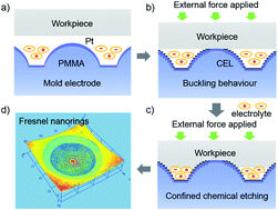
Can isotropic wet chemical etching be controlled with a spatial resolution at the nanometer scale, especially, for the repetitive microfabrication of hierarchical 3D μ-nanostructures on the continuously curved surface of functional materials? We present an innovative wet chemical etching method called “electrochemical buckling microfabrication”: first, a constant contact force is applied to generate a hierarchical 3D μ-nanostructure on a mold electrode surface through a buckling effect; then, the etchant is electrogenerated on-site and confined close to the mold electrode surface; finally, the buckled hierarchical 3D μ-nanostructures are transferred onto the surface of a GaxIn1−xP coated GaAs wafer through WCE. The concave microlens, with a Fresnel structure, has an enhanced photoluminescence at 630 nm. Comparing with energy beam direct writing techniques and nanoimprint lithography, this method provides an electrochemical microfabrication pathway for the semiconductor industry, with low cost and high throughput.
 Please wait while we load your content...

