Influence of the grain orientation on the charge transport properties of organic field-effect transistors†
Abstract
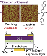
We report the effects of crystalline grain orientation on the charge transport properties of a J-aggregate bisazomethine dye (DE2) in thin films. Highly oriented DE2 organic field-effect transistors are fabricated using an insulating alignment layer of poly(tetrafluoroethylene) in the gate dielectric. An enhancement of about one and two orders of magnitude in hole mobility is achieved when the molecules and the crystalline grains are aligned perpendicular and parallel to the transistor channel, respectively. Ambipolar transport is observed only for the parallel alignment. To gain additional insights into the role of molecular packing on the charge transport properties of DE2, quantum chemical calculations are carried out to determine and compare the energetic splittings of the highest occupied molecular orbitals (HOMO) and of the lowest unoccupied molecular orbitals (LUMO) in the film. The results provide evidence that DE2 is intrinsically an ambipolar organic semiconductor and demonstrates the important role played by grain boundary orientation on charge trapping processes. Overall, the demonstration of field-effect mobilities as high as 0.01 cm2 V−1 s−1 and the observation of ambipolar transport in our devices represent an obvious milestone for the possible use of J-aggregate thin films in organic electronic devices. In addition, this work provides significant insights into the interplay between crystalline grain orientation and ambipolar charge transport properties in organic thin films.


 Please wait while we load your content...