
Superhigh out-of-plane piezoelectricity, low thermal conductivity and photocatalytic abilities in ultrathin 2D van der Waals heterostructures of boron monophosphide and gallium nitride†
 a
Ashima
Rawat,
a
Dimple,
a
Nityasagar
Jena,
a
Raihan
Ahammed
a
and
Abir
De Sarkar
*a
a
Ashima
Rawat,
a
Dimple,
a
Nityasagar
Jena,
a
Raihan
Ahammed
a
and
Abir
De Sarkar
*a
Abstract
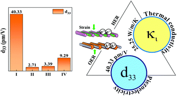
A stable 2D van der Waals (vdW) heterobilayer, constituted by boron monophosphide (BP) and Gallium Nitride (GaN) monolayers, has been explored for different kinds of energy conversion and nanoelectronics. The nearly matched lattice constants of GaN and BP are commensurate with each other in their lattice structures. The out-of-plane inversion asymmetry coupled with the large difference in atomic charges between the GaN and BP monolayers induces in the heterobilayer a giant out-of-plane piezoelectric coefficient (|d33|max ≈ 40 pm V−1), which is the highest ever reported in 2D materials of a finite thickness. It is much higher than the out-of-plane piezoelectric coefficient reported earlier in multilayered Janus transition metal dichalcogenide MXY (M = Mo, W; X, Y = S, Se, Te) (|d33|max = 10.57 pm V−1). Such a high out-of-plane piezoelectricity found in a BP/GaN heterobilayer can bring about gigantic strain-tunable top gating effects in nanopiezotronic devices based on the same. Moreover, electron mobility (∼104 cm2 V−1 s−1) is much higher than that of transition metal dichalcogenides and conventional semiconductors. The origin of low lattice thermal conductivity (κL ∼ 25.25 W m−1 K−1) in BP/GaN at room temperature, which is lower than that of black phosphorene (78 W m−1 K−1), buckled arsenene (61 W m−1 K−1), BCN (90 W m−1 K−1), MoS2 (34.5 W m−1 K−1) and WS2 (32 W m−1 K−1) monolayers, has been systematically investigated via phonon dispersion, lattice thermal conductivity, phonon lifetime and mode Grüneisen parameters. The valence band maximum (VBM) and conduction band minimum (CBM) arising from GaN and BP monolayers respectively result in a type II vdW heterobilayer, which is found to be thermodynamically favorable for photocatalytic water splitting in both acidic and neutral media. The exciton binding energies are comparable to those of MoS2 and C3N4 single layers, while the absorbance reaches as high as ∼105 cm−1 in the visible wavelength region. The emergence of high piezoelectricity, high carrier mobility, low lattice thermal conductivity and photocatalytic water splitting abilities in the proposed vdW heterobilayer signifies enormous potential for its versatile applications in nanoscale energy harvesting, e.g., nano-sensors in medical devices, future nanopiezotronics, 2D thermoelectrics and solar energy conversion.
- This article is part of the themed collection: Editor’s Choice: Computational studies of nanomaterials for energy, catalysis and electronics
 Please wait while we load your content...

