
Direct observation of an electrically degenerate interface layer in a GaN/sapphire heterostructure†

Abstract
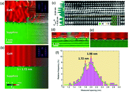
An electrically degenerate layer deteriorates the optoelectric performance of a wide band gap semiconductor grown on an insulator substrate. This detrimental effect can be passively avoided by using a buffer layer to harbor various lattice defects. However, the longstanding scientific questions regarding the microscopic origin of the degenerate interface layer and the effect of local changes in the atomic structure and chemical environment at an interface on the functionality of a desired film have remained unanswered. Moreover, this is key information for the development of ultrathin optoelectronic devices. In this study, we discuss the direct observation of a degenerate interface phase at the GaN/sapphire interface on an atomic scale. By combining high-resolution transmission electron microscopy and electron energy loss spectroscopy, we detect the presence of an ultrathin (∼6.5 Å) α-Ga2O3−x layer near the GaN/sapphire interface, which is subjected to ∼4.5% biaxial compressive strain and contains many oxygen vacancies. Density functional theory calculations show that the presence of a defective α-Ga2O3−x thin layer in the GaN and sapphire heterostructure remarkably reduces the band offset between the α-Ga2O3−x conduction band and the GaN valence band, thereby exerting a significant influence on the conductivity enhancement of the interface. Our results provide an unprecedented integrated picture of the degenerate interface phenomenon on an atomic scale, which would evolve the fundamental understanding about a wide band gap semiconductor heterostructure system.
 Please wait while we load your content...

