
Ultra-high light confinement and ultra-long propagation distance design for integratable optical chips based on plasmonic technology†

Abstract
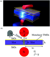
The ever-increasing demand for faster speed, broader bandwidth, and lower energy consumption of on-chip processing has motivated the use of light instead of electrons in functional communication components. However, considerable scattering loss severely affects the performance of nanoscale photonic devices when their physical sizes are smaller than the wavelength of light. Due to the tight localization of electromagnetic energy, plasmonic waveguides that work at visible and infrared wavebands have provided a solution for the optical diffraction limit problem and thus enable downscaling of optical circuits and chips at the nanoscale. However, due to the fundamental trade-off between propagation distance and light confinement, plasmonic waveguides, including conventional hybrid plasmonic waveguides (HPWGs), cannot be used as high performance integratable optical devices all the time. To solve this problem, a novel hybrid plasmonic waveguide is proposed where a hybrid metal-ridge-slot structure based on a two-dimensional (2D) transition metal dichalcogenide is embedded into two identical cylindrical dielectric waveguides. Benefiting from both the loss-less slot region and the high-index difference between the ultra-thin 2D material and the slot region, a 10 times longer propagation length and 100 times smaller mode area than the traditional HPWG are achieved at the telecommunication band. By removing the monolayer transition metal dichalcogenide, our designed waveguide shows a higher propagation length that is at least two orders of magnitude larger than its traditional HPWG counterpart. Therefore, the proposed hybridization waveguiding approach paves the way toward truly high-performance and deep-subwavelength integratable optical circuits and chips in the future.
 Please wait while we load your content...

