Non-destructive characterization of extended crystalline defects in confined semiconductor device structures†
 *a
Antoine
Pacco,
a
*a
Antoine
Pacco,
a
Abstract
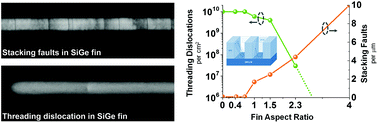
Semiconductor heterostructures are at the heart of most nanoelectronic and photonic devices such as advanced transistors, lasers, light emitting diodes, optical modulators and photo-detectors. However, the performance and reliability of the respective devices are often limited by the presence of crystalline defects which arise from plastic relaxation of misfit strain present in these heterogeneous systems. To date, characterizing the nature and distribution of such defects in 3D nanoscale devices precisely and non-destructively remains a critical metrology challenge. In this paper we demonstrate that electron channeling contrast imaging (ECCI) is capable of analyzing individual dislocations and stacking faults in confined 3D nanostructures, thereby fulfilling the aforementioned requirements. For this purpose we imaged the intensity of electrons backscattered from the sample under test under controlled diffraction conditions using a scanning electron microscope (SEM). In contrast to transmission electron microscopy (TEM) analysis, no electron transparent specimens need to be prepared. This enables a significant reduction of the detection limit (i.e. lowest defect density that can be assessed) as our approach facilitates the analysis of large sampling volumes, thereby providing excellent statistics. We applied the methodology to SiGe nanostructures grown by selective area epitaxy to study in detail how the nature and distribution of crystalline defects are affected by the dimensions of the structure. By comparing our observations with the results obtained using X-ray diffraction, TEM and chemical defect etching, we could verify the validity of the method. Our findings firmly establish that ECCI must be considered the method of choice for analyzing the crystalline quality of 3D semiconductor heterostructures with excellent precision even at low defect densities. As such, the technique aids in better understanding of strain relaxation and defect formation mechanisms at the nanoscale and, moreover, facilitates the development and fabrication of next generation nanoelectronic and photonic devices.
 Please wait while we load your content...

