Real-time atomic scale observation of void formation and anisotropic growth in II–VI semiconducting ribbons†
 *a
*a
Abstract
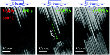
Void formation in semiconductors is generally considered to be deteriorating. However, for some systems, void formation and evolution are beneficial and can be used for the fabrication of novel nanostructures. In either scenario, the understanding of void formation and evolution is of both scientific and technical high importance. Herein, using ZnS ribbons as an example, we report real-time observations of void formation and the kinetics of growth at the nano- and atomic scales upon heating. Direct imaging reveals that voids, created by a focused electron beam in wurtzite (WZ) ribbons, have a rectangular shape elongated along the <0001> direction. The voids are enclosed by low-surface-energy planes including {01−10} and {2−1−10}, with minor contribution from the higher-energy {0001} planes. Driven by thermodynamics to minimize surface energy, the voids grow straight along the [000±1] directions, exhibiting a strong anisotropy. Occasionally, we observe oscillatory kinetics involving periodic void growth and shrinkage, likely due to the fluctuation of the local chemical potential leading to a transitional kinetic state. We also reveal that the morphology and growth kinetics of voids are highly structure-dependent. Real-time observation during void growth through the complex WZ–zinc blende (ZB)–WZ structure shows that the void, with an initial elongated rectangular morphology in the WZ domain, transforms into a different shape, dominated by the {110} surfaces, after migrating to a domain of the ZB structure. However, when the void moves from the ZB to the WZ domain, it transforms back into a rectangular shape followed by fast growth along the [0001] direction. Our experimental results, together with density functional theory (DFT) calculations, provide valuable insights into the mechanistic understanding of void formation and evolution in semiconductors. More importantly, our study may shed light on new pathways for the morphological modulation of nanostructures by utilizing the intrinsic anisotropy of void evolution in WZ semiconductors.
 Please wait while we load your content...

