Issue 33, 2016

Equal variations of the Fermi level and work function in graphene at the nanoscale

Abstract

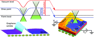
If surface effects are neglected, any change of the Fermi level in a semiconductor is expected to result in an equal and opposite change of the work function. However, this is in general not observed in three-dimensional semiconductors, because of Fermi level pinning at the surface. By combining Kelvin probe force microscopy and scanning tunneling spectroscopy on single layer graphene, we measure both the local work function and the charge carrier density. The one-to-one equivalence of changes in the Fermi level and the work function is demonstrated to accurately hold in single layer graphene down to the nanometer scale.

Graphical abstract: Equal variations of the Fermi level and work function in graphene at the nanoscale

Article information

Article type
Communication
Submitted
07 Jun 2016
Accepted
26 Jul 2016
First published
29 Jul 2016

Nanoscale, 2016,8, 15162-15166

Equal variations of the Fermi level and work function in graphene at the nanoscale

S. Samaddar, J. Coraux, S. C. Martin, B. Grévin, H. Courtois and C. B. Winkelmann, Nanoscale, 2016, 8, 15162 DOI: 10.1039/C6NR04606A

To request permission to reproduce material from this article, please go to the Copyright Clearance Center request page.

If you are an author contributing to an RSC publication, you do not need to request permission provided correct acknowledgement is given.

If you are the author of this article, you do not need to request permission to reproduce figures and diagrams provided correct acknowledgement is given. If you want to reproduce the whole article in a third-party publication (excluding your thesis/dissertation for which permission is not required) please go to the Copyright Clearance Center request page.

Read more about how to correctly acknowledge RSC content.

Social activity

Spotlight

Advertisements