Issue 37, 2015

Metal–insulator crossover in multilayered MoS2

Abstract

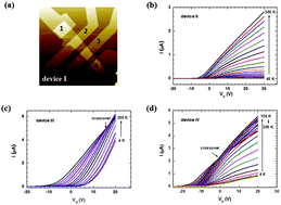
The temperature dependence of electrical transport properties was investigated for multilayered MoS2 field effect transistor devices with thicknesses of 3–22 nm. Some devices showed typical n-type semiconducting behavior, while others exhibited metal–insulator crossover (MIC) from metallic to insulating conduction at finite temperatures. The latter effect occurred near zero gate voltage or at high positive gate voltages. Analysis of Raman spectroscopy revealed the key difference that devices with MIC have a metallic 1T phase as well as a semiconducting 2H phase, whereas devices without the MIC did not have a metallic 1T phase. These results suggest that the metallic 1T phase may contribute to inducing the MIC.

Graphical abstract: Metal–insulator crossover in multilayered MoS2

Supplementary files

Article information

Article type
Communication
Submitted
03 Aug 2015
Accepted
25 Aug 2015
First published
27 Aug 2015

Nanoscale, 2015,7, 15127-15133

Author version available

Metal–insulator crossover in multilayered MoS2

M. J. Park, S. Yi, J. H. Kim and K. Yoo, Nanoscale, 2015, 7, 15127 DOI: 10.1039/C5NR05223H

To request permission to reproduce material from this article, please go to the Copyright Clearance Center request page.

If you are an author contributing to an RSC publication, you do not need to request permission provided correct acknowledgement is given.

If you are the author of this article, you do not need to request permission to reproduce figures and diagrams provided correct acknowledgement is given. If you want to reproduce the whole article in a third-party publication (excluding your thesis/dissertation for which permission is not required) please go to the Copyright Clearance Center request page.

Read more about how to correctly acknowledge RSC content.

Social activity

Spotlight

Advertisements