Issue 14, 2014

A mechanical and electrical transistor structure (METS) with a sub-2 nm nanogap for effective voltage scaling

Abstract

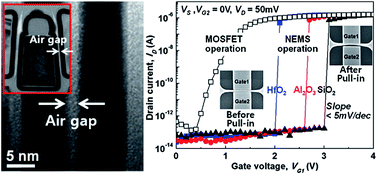
A mechanical and electrical transistor structure (METS) is proposed for effective voltage scaling. The sub-2 nm nanogap by atomic layer deposition (ALD) without stiction and the application of a dielectric with high-permittivity allowed the pull-in voltage of sub-2 V, showing the strength of the mechanical actuation that is hard to realize in a typical complementary metal–oxide–semiconductor (CMOS) transistor. The results are verified by simulation and interpreted by the numerical equation. Therefore the METS can pave a new way to make a breakthrough to overcome the limits of CMOS technology.

Graphical abstract: A mechanical and electrical transistor structure (METS) with a sub-2 nm nanogap for effective voltage scaling

Supplementary files

Article information

Article type
Communication
Submitted
25 Nov 2013
Accepted
20 Apr 2014
First published
22 Apr 2014

Nanoscale, 2014,6, 7799-7804

A mechanical and electrical transistor structure (METS) with a sub-2 nm nanogap for effective voltage scaling

B. Lee, D. Moon, H. Jang, C. Kim, M. Seol, J. Choi, D. Lee, M. Kim, J. Yoon and Y. Choi, Nanoscale, 2014, 6, 7799 DOI: 10.1039/C3NR06251A

To request permission to reproduce material from this article, please go to the Copyright Clearance Center request page.

If you are an author contributing to an RSC publication, you do not need to request permission provided correct acknowledgement is given.

If you are the author of this article, you do not need to request permission to reproduce figures and diagrams provided correct acknowledgement is given. If you want to reproduce the whole article in a third-party publication (excluding your thesis/dissertation for which permission is not required) please go to the Copyright Clearance Center request page.

Read more about how to correctly acknowledge RSC content.

Social activity

Spotlight

Advertisements