Issue 9, 2013

Room temperature deposition of nanostructured Bi2Se3 thin films for photoelectrochemical application: effect of chelating agents

Abstract

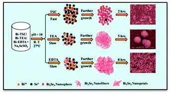
Nanostructured bismuth selenide (Bi2Se3) thin films have been deposited by chemical bath deposition method at room temperature using three different chelating agents, trisodium citrate, triethanolamine and ethylenedimminetetraacetic acid. The structural, morphological, optical and photoelectrochemical properties of Bi2Se3 thin films have been investigated as a function of different chelating agents. X-Ray diffraction studies revealed that the films were nanocrystalline in nature with a rhombohedral crystal structure. Trisodium citrate chelate resulted in Bi2Se3 thin films with poor crystallinity; further improvement in the crystallinity of the films was observed with triethanolamine and ethylenedimminetetraacetic acid chelates. From scanning electron microscopy, a uniform sphere-like morphology having an average sphere diameter of 90 nm was observed with trisodium citrate chelate. In the case of triethanolamine, a fibrous morphology with an average fiber thickness of 60 nm was observed, whereas for ethylenedimminetetraacetic acid chelate, a vertically arrayed petal-like morphology having petal thickness of 50–70 nm was observed. The UV-Vis absorption studies revealed that the band gap energy of the Bi2Se3 thin films with trisodium citrate, triethanolamine and ethylenedimminetetraacetic acid chelates was 1.55, 1.48 and 1.40 eV, respectively. The maximum short circuit current densities (Jsc) of 0.158, 0.214 and 0.284 mA cm−2 and the corresponding open circuit voltages (Voc) of 196, 206 and 217 mV were obtained with trisodium citrate, triethanolamine and ethylenedimminetetraacetic acid chelates, respectively. The Bi2Se3 thin films deposited using triethanolamine and ethylenedimminetetraacetic acid chelates show better photoelectrochemical performance as compared with trisodium citrate chelate.

Graphical abstract: Room temperature deposition of nanostructured Bi2Se3 thin films for photoelectrochemical application: effect of chelating agents

Article information

Article type
Paper
Submitted
03 May 2013
Accepted
20 Jun 2013
First published
16 Jul 2013

New J. Chem., 2013,37, 2821-2828

Room temperature deposition of nanostructured Bi2Se3 thin films for photoelectrochemical application: effect of chelating agents

S. D. Kharade, N. B. Pawar, V. B. Ghanwat, S. S. Mali, W. R. Bae, P. S. Patil, C. K. Hong, J. Kim and P. N. Bhosale, New J. Chem., 2013, 37, 2821 DOI: 10.1039/C3NJ00463E

To request permission to reproduce material from this article, please go to the Copyright Clearance Center request page.

If you are an author contributing to an RSC publication, you do not need to request permission provided correct acknowledgement is given.

If you are the author of this article, you do not need to request permission to reproduce figures and diagrams provided correct acknowledgement is given. If you want to reproduce the whole article in a third-party publication (excluding your thesis/dissertation for which permission is not required) please go to the Copyright Clearance Center request page.

Read more about how to correctly acknowledge RSC content.

Social activity

Spotlight

Advertisements