Issue 6, 2013

A post silicon-on-insulator compatible smart tube technology

Abstract

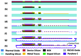
This paper reports a technology to fabricate micro-parylene tubes with integrated sensors. The unique advantage of this new technology is its ability to incorporate high-temperature solid-state materials. Standard CMOS and MEMS devices can be fabricated first on the silicon wafers and then the smart tubes are formed by taking advantage of XeF2 isotropic silicon etching and conformal parylene coating.

Graphical abstract: A post silicon-on-insulator compatible smart tube technology

Article information

Article type
Communication
Submitted
21 Nov 2012
Accepted
20 Dec 2012
First published
21 Dec 2012

Lab Chip, 2013,13, 1027-1030

A post silicon-on-insulator compatible smart tube technology

H. Tu and Y. Xu, Lab Chip, 2013, 13, 1027 DOI: 10.1039/C2LC41281K

To request permission to reproduce material from this article, please go to the Copyright Clearance Center request page.

If you are an author contributing to an RSC publication, you do not need to request permission provided correct acknowledgement is given.

If you are the author of this article, you do not need to request permission to reproduce figures and diagrams provided correct acknowledgement is given. If you want to reproduce the whole article in a third-party publication (excluding your thesis/dissertation for which permission is not required) please go to the Copyright Clearance Center request page.

Read more about how to correctly acknowledge RSC content.

Social activity

Spotlight

Advertisements