Surface functional group modification induced partial Fermi level pinning and ohmic contact at borophene–MoS2 interfaces†

Abstract
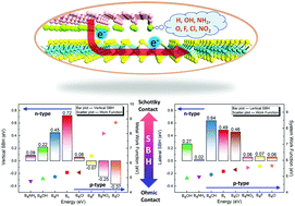
Large Schottky barrier at the electric contact interface drastically hinders the performance of two-dimensional (2D) semiconductor devices, because of which it is crucial to develop better methods to achieve the ohmic contact. Recently, a new field effect transistor (FET) device was constructed by the popular 2D channel material MoS2 and an electrode material borophene was detected theoretically, but the large Schottky barrier still existed. Hence, we used surface functional groups modification on the borophene surface to regulate this Schottky barrier, based on ab initio electronic structure calculations and quantum transport simulations. Our study shows that this method makes it possible to obtain tunable metal work functions in a wide range, and the ohmic contact can still be realized. Although van der Waals (vdW) contacts were observed at all the interfaces between the 2D borophene-based metals and the monolayer MoS2, the Fermi level pinning (FLP) effect was still obvious, and existed in our proposed system with the ohmic contact. Moreover, we also discuss the origin of the FLP with varying degrees. It was found that the interface dipole and metal-induced gap states (MIGS) would be responsible for the FLP of vertical and lateral directions, respectively. More precisely, we find that the size of MIGS is dependent on the relative orientation between the functional group and metal–MoS2 interface. This work not only suggests that surface functional group modification is effective in forming ohmic contact with MoS2, but also holds some implication in the fundamental research on metal–semiconductor contacts with the vdW type.
 Please wait while we load your content...

