Issue 18, 2007

Semiconductor and ceramic nanoparticle films deposited by chemical bath deposition

Abstract
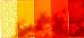
Chemical bath deposition (CBD) has been used to deposit films of metal sulfides, selenides and oxides, together with some miscellaneous compounds, beginning nearly 140 years ago. While it is a well-known technique in a few specific areas (notably photoconductive lead salt detectors, photoelectrodes and more recently, thin film solar cells), it is by and large an under-appreciated technique. The more recent interest in all things ‘nano’ has provided a boost for CBD: since it is a low temperature, solution (almost always aqueous) technique, crystal size is often very small. This is evidenced by the existence of size quantization commonly found in CBD semiconductor films. The intention of this review is to provide readers, many of whom may not even be aware of the CBD technique, with an overview of how the technique has been used to fabricate nanocrystalline semiconductor (this terminology also includes oxides often classified as ceramics) films and some properties of these films. The review begins, after a short introduction, with a general description of the CBD method, designed to give the reader a basic knowledge of the technique. The rest of the review then focuses on nanocrystalline (or, in the few cases of amorphous deposits, nanoparticle) films. The various factors which determine crystal size are first discussed. This is followed by some of the many examples of size quantization observed in the films. Since CBD films are usually porous, surface effects can be very important, and various surface-dependent properties (light emission and surface states) as well as surface modification, are treated: (although some properties, like emission, can be strongly dependent on both surface and ‘bulk’). Because of the fact that many CBD films have been made specifically for use as photoelectrodes in photoelectrochemical cells, there is next a chapter on this topic with a few examples of such photoelectrodes. Film structure and morphology follows with examples of patterning, porosity and crystal shape. The review concludes with some of the author’s opinions as to what the near future holds for CBD development in general.

Graphical abstract: Semiconductor and ceramic nanoparticle films deposited by chemical bath deposition

Article information

Article type
Invited Article
Submitted
14 Nov 2006
Accepted
20 Dec 2006
First published
09 Feb 2007

Phys. Chem. Chem. Phys., 2007,9, 2181-2196

Semiconductor and ceramic nanoparticle films deposited by chemical bath deposition

G. Hodes, Phys. Chem. Chem. Phys., 2007, 9, 2181 DOI: 10.1039/B616684A

To request permission to reproduce material from this article, please go to the Copyright Clearance Center request page.

If you are an author contributing to an RSC publication, you do not need to request permission provided correct acknowledgement is given.

If you are the author of this article, you do not need to request permission to reproduce figures and diagrams provided correct acknowledgement is given. If you want to reproduce the whole article in a third-party publication (excluding your thesis/dissertation for which permission is not required) please go to the Copyright Clearance Center request page.

Read more about how to correctly acknowledge RSC content.

Social activity

Spotlight

Advertisements