Issue 6, 2017

Thick GaN growth via GaN nanodot formation by HVPE

Abstract

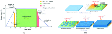
We demonstrate a 400 μm-thick GaN layer on 4 inch (0001) Al2O3 substrates through GaN nanodot formation as a seed for stress relaxation layers, which were formed by an in situ special surface treatment using HVPE. The size and density of the GaN nanodots determined the thickness of the stress relaxation layers and the structural properties of thick GaN. The 400 μm-thick GaN layer exhibits a smooth surface and high crystal quality with FWHM of 104 arcsec and 163 arcsec in the (002) and (102) X-ray rocking curves, respectively. The dislocation density estimated via micro-PL measurements was 2 × 106 cm−2. This can provide an efficient and simple way to fabricate thick GaN layers on an Al2O3 substrate without ex situ buffer layer formation or additional complicated processes.

Graphical abstract: Thick GaN growth via GaN nanodot formation by HVPE

Supplementary files

Article information

Article type
Paper
Submitted
05 Oct 2016
Accepted
28 Nov 2016
First published
29 Nov 2016

CrystEngComm, 2017,19, 930-935

Thick GaN growth via GaN nanodot formation by HVPE

M. Lee, D. Mikulik and S. Park, CrystEngComm, 2017, 19, 930 DOI: 10.1039/C6CE02125E

To request permission to reproduce material from this article, please go to the Copyright Clearance Center request page.

If you are an author contributing to an RSC publication, you do not need to request permission provided correct acknowledgement is given.

If you are the author of this article, you do not need to request permission to reproduce figures and diagrams provided correct acknowledgement is given. If you want to reproduce the whole article in a third-party publication (excluding your thesis/dissertation for which permission is not required) please go to the Copyright Clearance Center request page.

Read more about how to correctly acknowledge RSC content.

Social activity

Spotlight

Advertisements