Issue 27, 2013

Micro-patterned ZnO semiconductors for high performance thin film transistors via chemical imprinting with a PDMS stamp

Abstract

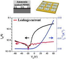
Chemical imprinting was conducted on ZnO semiconductor films via a chemical reaction at the contact regions between a micro-patterned PDMS stamp and ZnO films. In addition, we applied the chemical imprinting on Li doped ZnO thin films for high performance TFTs fabrication. The representative micro-patterned Li doped ZnO TFTs showed a field effect mobility of 4.2 cm2 V−1 s−1 after sintering at 300 °C.

Graphical abstract: Micro-patterned ZnO semiconductors for high performance thin film transistors via chemical imprinting with a PDMS stamp

Supplementary files

Article information

Article type
Communication
Submitted
06 Nov 2012
Accepted
06 Feb 2013
First published
07 Feb 2013

Chem. Commun., 2013,49, 2783-2785

Micro-patterned ZnO semiconductors for high performance thin film transistors via chemical imprinting with a PDMS stamp

K. Seong, K. Kim, S. Y. Park and Y. S. Kim, Chem. Commun., 2013, 49, 2783 DOI: 10.1039/C3CC38021A

To request permission to reproduce material from this article, please go to the Copyright Clearance Center request page.

If you are an author contributing to an RSC publication, you do not need to request permission provided correct acknowledgement is given.

If you are the author of this article, you do not need to request permission to reproduce figures and diagrams provided correct acknowledgement is given. If you want to reproduce the whole article in a third-party publication (excluding your thesis/dissertation for which permission is not required) please go to the Copyright Clearance Center request page.

Read more about how to correctly acknowledge RSC content.

Social activity

Spotlight

Advertisements