Nanoscale electrochemical 3D deposition of cobalt with nanosecond voltage pulses in an STM†

Abstract
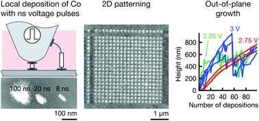
To explore a minimal feature size of <100 nm with electrochemical additive manufacturing, we use a strategy originally applied to microscale electrochemical machining for the nanoscale deposition of Co on Au. The concept's essence is the localization of electrochemical reactions below a probe during polarization with ns-long voltage pulses. As shown, a confinement that exceeds that predicted by a simple model based on the time constant for one-dimensional double layer charging enables a feature size of <100 nm for 2D patterning. We further indirectly verify the potential for out-of-plane deposition by tracking growth curves of high-aspect-ratio deposits. Importantly, we report a lack of anodic stability of Au tips used for patterning. As an inert probe is the prerequisite for controlled structuring, we experimentally verify an increased resistance of Pt probes against degradation. Consequently, the developed setup and processes show a path towards reproducible direct 2D and 3D patterning of metals at the nanoscale.
 Please wait while we load your content...

