A route to engineered high aspect-ratio silicon nanostructures through regenerative secondary mask lithography†
Abstract
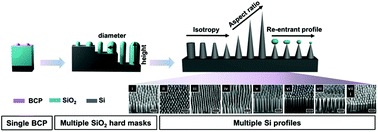
Silicon nanostructuring imparts unique material properties including antireflectivity, antifogging, anti-icing, self-cleaning, and/or antimicrobial activity. To tune these properties however, a good control over features’ size and shape is essential. Here, a versatile fabrication process is presented to achieve tailored silicon nanostructures (thin/thick pillars, sharp/truncated/re-entrant cones), of pitch down to ∼50 nm, and high-aspect ratio (>10). The approach relies on pre-assembled block copolymer (BCP) micelles and their direct transfer into a glass hard mask of an arbitrary thickness, now enabled by our recently reported regenerative secondary mask lithography. During this pattern transfer, not only can the mask diameter be decreased but also uniquely increased, constituting the first method to achieve such tunability without necessitating a different molecular weight BCP. Consequently, the hard mask modulation (height, diameter) advances the flexibility in attainable inter-pillar spacing, aspect ratios, and re-entrant profiles (= glass on silicon). Combined with adjusted silicon etch conditions, the morphology of nanopatterns can be highly customized. The process control and scalability enable uniform patterning of a 6-inch wafer which is verified through cross-wafer excellent antireflectivity (<5%) and water-repellency (advancing contact angle 158°; hysteresis 1°). The implementation of this approach to silicon nanostructuring is envisioned to be far-reaching, facilitating fundamental studies and targeting applications spanning solar panels, antifogging/antibacterial surfaces, sensing, amongst many others.


 Please wait while we load your content...