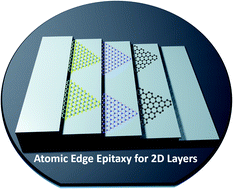
Wafer-scale single-orientation 2D layers by atomic edge-guided epitaxial growth
Abstract
Two-dimensional (2D) layered materials hold tremendous promise for post-Si nanoelectronics due to their unique optical and electrical properties. Significant advances have been achieved in device fabrication and synthesis routes for 2D nanoelectronics over the past decade; however, one major bottleneck preventing their immediate applications has been the lack of a reproducible approach for growing wafer-scale single-crystal films despite tremendous progress in recent experimental demonstrations. In this tutorial review, we provide a systematic summary of the critical factors—including crystal/substrate symmetry and energy consideration—necessary for synthesizing single-orientation 2D layers. In particular, we focus on the discussions of the atomic edge-guided epitaxial growth, which assists in unidirectional nucleation for the wafer-scale growth of single-crystal 2D layers.


 Please wait while we load your content...