
Emerging negative differential resistance effects and novel tunable electronic behaviors of the broken-gap KAgSe/SiC2 van der Waals heterojunction†

Abstract
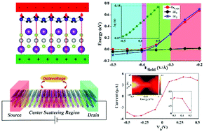
KAgSe is a newly discovered two-dimensional (2D) layered material, which shows great performance in optical absorption and potential applications as a favorable optical electronic device. However, its band gap is independent of the layer numbers, which restricts its further application in the field of tunneling field effect transistor (TFET). To address this issue, by integrating 2D KAgSe with a substrate of 2D penta-SiC2, a 2D KAgSe/SiC2 vertical van der Waals heterojunction (vdWH) is proposed to extend the application of 2D KAgSe, and its structural, electronic and quantum transport behaviors are systematically investigated by using the first-principles method. Firstly, the robust structural stability of this vdWH is verified by evaluating its formation energy, vibrational phonon spectrum and molecular dynamics at high temperature. Moreover, various new functionalities are found for this novel 2D vdWH, which displays a relatively unique type-III band alignment and implies favorable application in TFETs considering the band-to-band tunneling process. The ideal electronic features of the vdWH can also be modulated by various external parameters including in-plane strain, interfacial distance, and external electric field. Especially under increasing negative external electric field, phase transitions occur for the vdWH from type-III band alignment to type-II, and then type-I and finally Schottky contact accompanied by the decrease of charge transfer and the reversal of net electric field in the interfacial region. Furthermore, quantum transport properties are investigated for a 2D KAgSe/SiC2 vdWH based two-probe nano-device, and a sizable negative differential resistance (NDR) effect is obtained. Interestingly, the NDR effect is mainly dominated by the bias related band alignments in both leads associated with the mismatch of the conducting channel in the leads and scattering region, which is fundamentally different from the mechanism of general TFETs reported in previous publications where the NDR effect is mainly induced by the energy renormalization of the center material. The complete new mechanism of NDR effects in KAgSe/SiC2 vdWH may provide a new strategy for the experimental design of future TFETs. We believe that the fascinating 2D KAgSe/SiC2 vdWH can not only extend the application range of 2D KAgSe, but also inspire intensive research studies on the engineering of multi-functional nanoelectronic devices in the near future.
 Please wait while we load your content...

