
Template effects in Cu(i)–Bi(iii) iodide double perovskites: a study of crystal structure, film orientation, band gap and photocurrent response†

Abstract
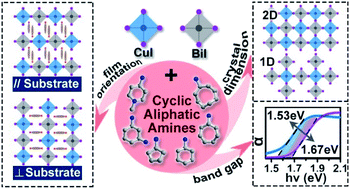
The toxicity of lead has inspired recent interest in making lead-free photovoltaic materials, among which the bimetallic double perovskite (DP) strategy is very promising. Unlike the popular Ag(I)–Bi(III) based DPs with wider band gaps ∼2.0 eV, in our previous study we found that the Cu(I)–Bi(III) method may have narrower band gaps ∼1.6 eV. Here we expand this strategy to various amines, from which we can see that the cyclic aliphatic amines (CAAs) are critical to govern the structural dimensions, thin film orientations and band gaps of the Cu(I)–Bi(III) iodide DPs. Among these compounds, CAAs with a “Z-shape” and six-member-rings result in two-dimensional structures (compounds 1–5), while CAAs with a “C-shape” and five-member-rings result in 1D bimetallic chains (compounds 6 and 7). Regardless of the structural dimensions, all seven compounds show narrow band gaps between 1.53 and 1.67 eV, which can be correlated to the distortions of the Cu–I–Bi angles. The band gap will be narrower if the Cu–I–Bi angle is closer to 180° or the octahedral distortion is smaller. Moreover, DFT calculations reveal that such band gaps are flat and direct in nature. Interestingly, the thin films formed by these compounds show preferential orientations to the ITO substrate with respect to the symmetries of the amines. For mirror-symmetric diamines the inorganic layers tend to be perpendicular to ITO; for asymmetric diamines the inorganic layers tend to be randomly oriented on ITO; for the asymmetric mono-amines the inorganic layers tend to be parallel to ITO. Such a phenomenon is, as far as we know, unknown to the field of perovskite thin film construction. To further reveal the potential of these materials for photovoltaic application we took compound 3 as a representative to study the photoelectric properties. From 20 °C to 130 °C, the conductivity of compound 3 increases over five orders of magnitude, ramping from 3.97 × 10⁻¹⁰ S cm−1 to 2.78 × 10⁻⁵ S cm−1, indicating a formal semiconducting behaviour. Thus, the photo-current response experiments show a ca. 17.5 nA difference between Ilight and Idark for 3, indicating the potential application of this material for light harvesting.
 Please wait while we load your content...

