
Photolithography in the vacuum ultraviolet (172 nm) with sub-400 nm resolution: photoablative patterning of nanostructures and optical components in bulk polymers and thin films on semiconductors
 *abc
Jinhong
Kim,
ab
*abc
Jinhong
Kim,
ab
Abstract
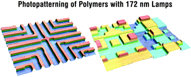
Precision photoablation of bulk polymers or films with incoherent vacuum ultraviolet (VUV) radiation from flat, microplasma array-powered lamps has led to the realization of a photolithographic process in which an acrylic, polycarbonate, or other polymer serves as a dry photoresist. Patterning of the surface of commercial-grade, bulk polymers (or films spun onto Si substrates) such as poly-methyl methacrylate (PMMA) and acrylonitrile butadiene styrene (ABS) with 172 nm lamp intensities as low as ∼10 mW cm−2 and a fused silica contact mask yields trenches, as well as arbitrarily-complex 3D structures, with depths reproducible to ∼10 nm. For 172 nm intensities of 10 mW cm−2 at the substrate, linearized PMMA photoablation rates of ∼4 nm s−1 are measured for exposure times t ≤ 70 s but a gradual decline is observed thereafter. Beyond t ∼ 300 s, the polymer removal rate gradually saturates at ∼0.2 nm s−1. Intricate patterns are readily produced in bulk acrylics or 40–200 nm thick acrylic films on Si with two or more exposures and overall process times of typically 10–300 s. The photoablation process is sufficiently precise that the smallest lateral feature size fabricated reproducibly to date, ∼350 nm, appears to be limited primarily by the photomask itself. Examples of the versatility and precision of this photolithographic process include the fabrication of arrays of aluminum nanomirrors, each atop a 350 nm or 1 μm-diameter Si post, as well as optical components such as transmission gratings or Fresnel lenses photoablated into PMMA.
- This article is part of the themed collection: 2020 Nanoscale HOT Article Collection
 Please wait while we load your content...

