Effect of an electric field during the deposition of silicon dioxide thin films by plasma enhanced atomic layer deposition: an experimental and computational study†
 a
Tahsin
Faraz,
c
W. M. M. (Erwin)
Kessels,
c
Felix
Otto,
e
Torsten
Fritz,
e
Marco
Gruenewald,
e
Klaus D.
Jandt,
f
Marek
Sierka
*b
and
Adriana
Szeghalmi
*ad
a
Tahsin
Faraz,
c
W. M. M. (Erwin)
Kessels,
c
Felix
Otto,
e
Torsten
Fritz,
e
Marco
Gruenewald,
e
Klaus D.
Jandt,
f
Marek
Sierka
*b
and
Adriana
Szeghalmi
*ad
Abstract
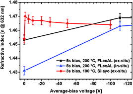
The growth, chemical, structural, mechanical, and optical properties of oxide thin films deposited by plasma enhanced atomic layer deposition (PEALD) are strongly influenced by the average-bias voltage applied during the reaction step of surface functional groups with oxygen plasma species. Here, this effect is investigated thoroughly for SiO2 deposited in two different PEALD tools at average-bias voltages up to −300 V. Already at a very low average-bias voltage (< −10 V), the SiO2 films have significantly lower water content than films grown without biasing together with the formation of denser films having a higher refractive index and nearly stoichiometric composition. Substrate biasing during PEALD also enables control of mechanical stress. The experimental findings are supported by density functional theory and atomistic simulations. They demonstrate that the application of an electric field during the plasma step results in an increased energy transfer between energetic ions and the surface, directly influencing relevant surface reactions. Applying an electric field during the PEALD process leads to SiO2 thin films with significantly improved properties comparable to films grown by ion beam sputtering.
 Please wait while we load your content...

