Ordered-vacancy-enabled indium sulphide printed in wafer-scale with enhanced electron mobility†
Abstract
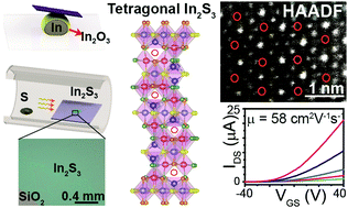
Metal chalcogenides are important members of the two-dimensional (2D) materials family and have been extensively investigated for high-performance electronic device applications. However, when they are produced on a large-scale, their carrier mobilities are strongly influenced by the surface conditions. Here, we print indium sulphide (In2S3) with the thickness down to the single unit cell limit on wafer-scale out of metallic indium liquid, in which structural indium vacancies are formed in an orderly fashion. First principles investigations reveal that the unique ordered-vacancy structure results in a highly dispersive conduction band with low effective electron mass, forming multiple band-like electronic transport channels sandwiched within the crystal structure which are less influenced by the surface conditions. Back-gated field effect transistors are fabricated, and the measured mobility is up to 58 cm2 V−1 s−1 with a high degree of reproducibility, which is amongst one of the highest reported for wafer-scale-grown ultra-thin metal chalcogenides. This establishes ordered-vacancy-enabled semiconductors in the 2D geometry as suitable alternatives for new generation high-performance electronic devices.


 Please wait while we load your content...