Transmission electron microscopy characterization of low temperature boron doped silicon epitaxial films
 *abc
Pere
Roca i Cabarrocas,
cd
*abc
Pere
Roca i Cabarrocas,
cd
Abstract
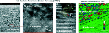
Transmission electron microscopy (TEM) techniques can provide a complementary understanding of the physico-chemical mechanisms of the growth and the annealing behavior of boron-doped hydrogenated silicon epitaxial films grown at low temperatures (<200 °C) by radio frequency plasma enhanced chemical vapor deposition (RF-PECVD). Compared to the standard boron diffusion or ion implantation, the PECVD process ensures a lower thermal budget and the realization of a sharper doping profile. The complexity of this epi-layer process lies on the fact that many impurities are incorporated during growth and their analysis requires the use of advanced characterization methods. Particular attention is paid to defects by combining high resolution transmission electron microscopy (HRTEM) and an image processing routine called geometric phase analysis (GPA) which allows the strain field to be studied. For the as-grown epitaxial layer, we will show how the non-conventional PECVD growth process influences its microstructure and gives it a non-uniform strain-field. In the annealed epitaxial layer, no strain is measured but nanotwins have been detected and analyzed through a geometric model. Scanning TEM (STEM) techniques are also applied to analyze chemical variation at the interface. A darker contrast is observed at the interface of the annealed sample most likely due to the migration of hydrogen atoms during annealing.
 Please wait while we load your content...

