A solvent-free and vacuum-free melt-processing method to fabricate organic semiconducting layers with large crystal size for organic electronic applications†

Abstract
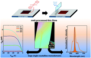
We report on an improved melt-processing method to prepare organic semiconducting layers with large crystal size and enhanced charge carrier mobilities. The organic compound used in this work is a solution-processable oligo(p-phenylene vinylene) derivative substituted at both ends with pyrene moieties. Accurate control of the temperature during the recrystallization of this compound from the melt enables the formation of large single crystal monodomains in thin films. The melt-processed organic layer shows higher mobilities in transistor configuration than in spin-coated films, which can be attributed to the presence of large-size crystalline monodomains as evidenced by X-ray diffraction measurements. We also investigated the photophysical properties of this material in spin-coated and melted films and found an increase of the photoluminescence quantum yield with the size of the crystals in the organic layer. The advantage of this method over the spin coating also allowed observation of amplified spontaneous emission that was only achieved in the melted film due to its improved luminescence efficiency. Overall, this study demonstrates a simple and versatile method, which does not require the use of any solvent and vacuum, to fabricate organic layers with large crystal size, suitable for the realization of organic electronic and light-emitting devices.
 Please wait while we load your content...

