Plasma-enhanced atomic-layer-deposited gallium nitride as an electron transport layer for planar perovskite solar cells†
Abstract
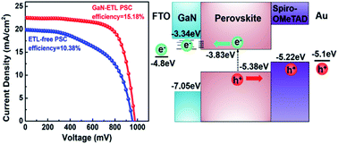
Low-temperature deposited gallium nitride (GaN) thin-films have been introduced into planar perovskite solar cells (PSCs) as electron transport layers (ETLs) for the first time. Compact and amorphous n-type GaN layers were uniformly coated on fluorine-doped tin oxide (FTO) glass substrates via plasma-enhanced atomic layer deposition (PEALD) technology, in which an optimized deposition temperature of 280 °C was identified and adopted. The as-prepared GaN thin-films were subsequently employed to fabricate planar PSCs with the device configuration FTO/GaN/perovskite/spiro-OMeTAD/Au. Interestingly, although a conduction-band-minimum (CBM) mismatch of 0.59 eV is found at the interface of the 50-PEALD-cycle GaN/perovskite, a significantly enhanced device efficiency from 10.38% to 15.18% has also been achieved relative to the ETL-free PSCs. Meanwhile, the current–voltage hysteresis and device stability of GaN-based PSCs can be remarkably improved. It is found that the GaN layer can promote the electron extraction and reduce recombination at the FTO/perovskite interface. This work demonstrates the feasibility and potential of GaN films as ETLs in planar PSCs.


 Please wait while we load your content...