Precise control of the microstructural, optical, and electrical properties of ultrathin Ga2O3 film through nanomixing with few atom-thick SiO2 interlayer via plasma enhanced atomic layer deposition
Abstract
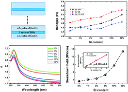
Ultrathin Ga2O3 films nanomixed with few atom-thick SiO2 interlayer were deposited on silicon and quartz substrates through plasma-enhanced atomic layer deposition. Upon adjusting the number of SiO2 atomic layers, different Si doping levels in Ga2O3 films were obtained. Herein, we report for the first time the use of this method to investigate the doping effect and realize the precise control of the microstructural, optical, and electrical properties of the Ga2O3 films. The experimental results indicated that the microstructural properties such as density, roughness, and chemical composition of the films are all affected by the number of doped SiO2 atomic layers. As the Si doping concentration increased in the films, the refractive index of the Ga2O3 films decreased monotonically, the optical transparency improved, and the average transmittances were >95% from ultraviolet to visual wavelengths for all the Si-doped Ga2O3 films. Moreover, the energy band-gap increased with the increase in Si composition, increasing from ∼4.8 eV for the undoped film to ∼5.1 eV for the film with a 20 at% Si doping level. Moreover, the breakdown field of the Ga2O3 film linearly improved from 6.8 MV cm−1 to 10.7 MV cm−1 as a function of the Si content. More importantly, this result enlightened us that the breakdown field of the Ga2O3 film can be further improved by increasing the Si doping concentration. This study provides a means to expand the properties of the new doped films and develop Ga2O3 film-based devices, such as transparent electrodes, photodetectors, thin film transistors, or high-power high-voltage devices.


 Please wait while we load your content...