The effect of N,N-dimethylformamide on MAPbI3 nanowires for application in flexible photodetectors†
Abstract
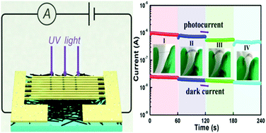
Owing to good crystal structure and novel one-dimensional (1D) outer surface, MAPbI3 nanowires (NWs) show fewer grain boundaries, lower defect density and longer carrier lifetime as compared with their polycrystalline thin films, leading to MAPbI3 NWs exhibiting higher quantum efficiencies in optoelectronic devices. Herein, by a simple two-step spin-coating method with the addition of various N,N-dimethylformamide (DMF) contents, a PbI2–DMF adduct is formed; this changes the micro-morphology of MAPbI3 perovskite from 3 dimensional (3D) nanocubic to 1D NW. Through optimizing the DMF contents, MAPbI3 NWs with strongest light absorbability and best crystallinity have been obtained (500 μL DMF). In addition, photodetectors (PDs) are assembled with various DMF amounts on glass substrates, and the optimal MAPbI3 NW PD (500 μL DMF) shows the best performance with on/off ratio greater than 250; the rise and decay times are 12 and 22 ms, respectively. Furthermore, a flexible MAPbI3 NW PD is assembled, and it shows good sequential and stable response with the on/off ratio of more than 45. Notably, under various bending curvatures and many cycles, the performance of the flexible NW device has only slight degradation. Our results may have great value for the application of flexible MAPbI3 NW devices in the future.


 Please wait while we load your content...