High carrier mobility in monolayer CVD-grown MoS2 through phonon suppression†
 ‡a
‡a
Abstract
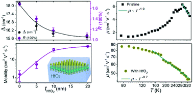
Mobility engineering is one of the most important challenges that determine the optoelectronic performance of two-dimensional (2D) materials. So far, charged-impurity scattering and electrical-contact barriers have been suppressed through high-κ dielectrics and seamless contact engineering, giving rise to carrier-mobility improvement in exfoliated 2D semiconducting MoS2. Here we demonstrate a facile and scalable technique to effectively suppress both Coulomb scattering and electron–phonon scattering via the HfO2 overlayer, resulting in a large mobility improvement in CVD-grown monolayer MoS2, in excess of 60 cm2 V−1 s−1. Surface passivation and suppression of Coulomb scattering can partially contribute to the mobility increase. Interestingly, we correlate the mobility increase with phonon quenching through Raman and temperature-dependent mobility measurements. The experimental method is facile, industrially scalable, and renders phonon engineering an additional leverage towards further improvements in 2D semiconductor mobility and device performance.
 Please wait while we load your content...

