Cryogenically probing the surface trap states of single nanowires passivated with self-assembled molecular monolayers†
Abstract
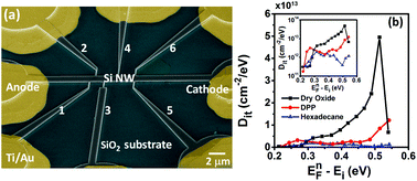
Optoelectronically probing the trap state density of single nanoscale devices is a powerful in situ nondestructive technique that is of significance for developing high gain photoconductors by surface engineering. However, the previously demonstrated optoelectronic methods are based on the exponential transient photoresponse assumption and only trap states in a very narrow bandgap region can be probed. In this Letter, we demonstrate a cryogenic technique that is capable of measuring the density of surface trap states in the full half bandgap without the exponential transient photoresponse assumption. The technique is applied to an array of silicon nanowire photoconductors that are fabricated on silicon-on-insulator (SOI) wafer by the top-down approach. Diethyl 1-propylphosphonate (DPP) and hexadecane molecular monolayers are self-assembled on silicon nanowire surfaces as the passivation layer in comparison with dry oxide passivation. The surface trap state density of the dry oxide passivated nanowires exponentially increases from the bandgap center, reaching a peak of ∼5 × 1013 cm−2 eV−1 at 50 meV below the conduction band. The defect state density is significantly suppressed after DPP and hexadecane molecules are grafted onto the nanowire surfaces via covalent bonds. The experimental observations are consistent with the density functional theory calculations.


 Please wait while we load your content...