Emerging photonic architectures in two-dimensional opto-electronics
Abstract
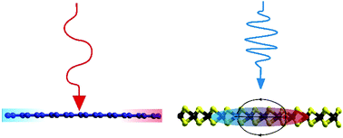
The isolation of thermodynamically stable, free standing materials with single to few atom thicknesses has brought about a revolution in materials science, condensed matter physics and device engineering for opto-electronic applications. These two dimensional (2D) materials cover a broad range of electronic properties ranging from zero-band gap, semi-metallic graphene to wide band gap semiconductors in sulfides and selenides of Mo and W to metallic behavior in Ti, Nb and Ta sulfides and selenides. This permits their potential application in opto-electronic devices from terahertz frequencies up to the ultraviolet portion of the spectrum. However, their atomically thin nature poses fundamental challenges in driving efficient light–matter interactions. A range of strategies have been explored from the area of photonics and resonant optics that enhance the coupling and interaction of light with atomically thin layers to overcome this challenge. By comparing and contrasting critical advantages of integrating nanophotonic elements with 2D materials, this review highlights the challenges and advantages of such opto-electronic devices.

- This article is part of the themed collection: 2D nanomaterials: graphene and transition metal dichalcogenides


 Please wait while we load your content...