New insights into the origin of hysteresis behavior in perovskite solar cells†
Abstract
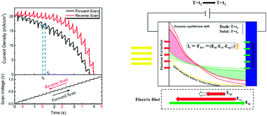
Perovskite solar cells (PSCs) have received tremendous attention due to their stunning progress in photovoltaic performance. The hysteresis behavior, however, is one of the major concerning issues accompanying the development of PSCs. In this context, we propose a new mechanism that explains the origin of hysteresis behavior by analyzing the electrical processes after changing the external electrical bias: the compensating electric field to the scanning voltage induced by drifting carriers. This is further verified by experiments, where we observed much reduced hysteresis in the current density–voltage (J–V) characteristics for the PSCs based on a thinner perovskite layer, which is a result of more evenly distributed electrons and holes. Moreover, light illumination with different wavelengths was applied to vary the initial carrier distribution inside the perovskite layer. We found that J–V curves when illuminating the device with longer wavelengths exhibited diminished hysteresis, which could be a result of more evenly generated carriers due to a smaller absorptivity than that with short wavelength illumination. Based on the proposed model, three key factors affecting the hysteresis behavior were pointed out, including the initial carrier distribution, the carrier transport properties in the perovskite layer, and the carrier extraction properties at the interfaces. Strategies to construct hysteresis-free and stable PSCs have thus been accordingly proposed.


 Please wait while we load your content...