Two-step synthesis and characterization of vertically stacked SnS–WS2 and SnS–MoS2 p–n heterojunctions†
Abstract
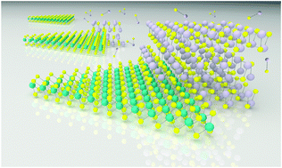
We demonstrate the synthesis of unique heterostructures consisting of SnS and WS2 (or SnS and MoS2) by two-step chemical vapor deposition (CVD). After the first CVD growth of triangular WS2 (MoS2) grains, the second CVD step was performed to grow square SnS grains on the same substrate. We found that these SnS grains can be grown at very low temperature with the substrate temperature of 200 °C. Most of the SnS grains nucleated from the side edges of WS2 (MoS2) grains, resulting in the formation of partly stacked heterostructures with a large overlapping area. The SnS grains showed doped p-type transfer character with a hole mobility of 15 cm2 V−1 s−1, while the WS2 and MoS2 grains displayed n-type character with a high on/off ratio of >106. The SnS–WS2 and SnS–MoS2 heterostructures exhibited clear rectifying behavior, signifying the formation of p–n junctions at their interfaces. This heterostructure growth combined with the low temperature SnS growth will provide a promising means to exploit two-dimensional heterostructures by avoiding possible damage to the first material.

- This article is part of the themed collection: 2018 PCCP HOT Articles


 Please wait while we load your content...