Solution grown double heterostructure on a large hybrid halide perovskite crystal†
Abstract
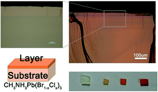
Heterostructure is playing a crucial role in current optoelectronic applications. Realizing the heterostructure in a recently exciting semiconductor material: hybrid halide perovskite crystals, has been a long-sought goal in the field. Here, we demonstrate modulation-doped layer growth on large hybrid halide perovskite crystals. We show that the well known problem of halide ion inter-diffusion can be controlled by (1) using low halide composition gradient and (2) adjusting solution concentrations just above the critical supersaturation, in the solvothermal liquid-phase growth process. In comparison to a few seconds dipping time previously reported for the ion-exchange processes, our layer growth time could be conveniently extended up to 80 minutes to grow a uniform and controllable layer, with a very thin inter-diffusion region. The growth of the CH3NH3PbBr3 layer on top of the CH3NH3Pb(Br0.85Cl0.15)3 bulk substrate is studied for different growth times to obtain up to a 30 μm layer thickness. The ion diffusion profile and layer thickness are verified, respectively, by cross-sectional characterization using scanning electron microscopy (SEM), energy dispersive spectroscopy (EDS). Electron back-scattering diffraction (EBSD) suggests a similar crystallographic orientation for both substrate and grown layers. Our diffusion model illustrates the halide ion concentration at the interface, correlating with the EDS mapping results. Optical imaging and photoluminescence (PL) characterization confirm the quality and bandgap of the grown layers. Especially, the growth process is further extended for two consecutive layers to create a double heterostructure for the first time with a large perovskite crystal. Our low cost process could pave the way for many optoelectronic applications such as color tunable light emitting diodes or photodetectors developed with perovskite crystals.


 Please wait while we load your content...