Facile growth of density- and diameter-controlled GaN nanobridges and their photodetector application†
Abstract
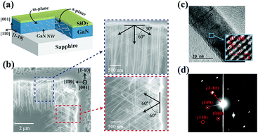
The growth of arrayed GaN nanobridges (NBs) and their application in a photodetector (PD) were studied. First, GaN nanowires (NWs) were selectively grown on the sidewalls of a GaN mesa using an Au catalyst-assisted vapor–liquid–solid (VLS) method, while their density was conveniently controlled by varying the dilution of the Au nanoparticle colloidal solution. It was revealed that an m-axis NW was preferentially fabricated on both the m-plane and a-plane sidewalls. A two-step VLS–VS growth technique was utilized for the radial core–shell structure composed of GaN, InGaN and InGaN/GaN multi-quantum wells (MQWs) that allowed independent control of the NW diameter. Finally, core–shell NBs were fabricated across a trench formed between two GaN mesas to be used as a light absorbing medium in a photoconductor. Their optical response was measured at various wavelengths and InGaN/GaN MQWs embedded in the core–shell structure exhibited an enhanced photoresponse to visible light.


 Please wait while we load your content...