Laser annealing of electrodeposited CuInSe2 semiconductor precursors: experiment and modeling†
 *a
*a
Abstract
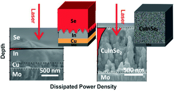
Laser annealing can reduce the annealing time required to form Cu(In,Ga)(S,Se)2 (CIGSe) thin films for use in thin film photovoltaics to a single second timescale, if not faster. In this work, we use microstructural characterization coupled with modeling of the optical and thermal properties to understand the laser annealing of three types of electrodeposited precursor stacks for the CIGSe parent compound CuInSe2. The precursor films are: stacked elemental layers Cu/In/Se, stacked binary selenides In2Se3/Cu2−xSe, and a single layer of coelectrodeposited Cu–In–Se. Conceptually, these stacks are ordered in terms of decreasing stored chemical and interfacial potential free energy, consideration of which predicts that the formation of large grained CuInSe2 from the stacked elemental layers would be the most exothermic and thus most rapid process. However we find that microstructural details of the electrodeposited films such as void fraction present in the stacked binary selenides dramatically alter the heat and mass flow. Additionally, modeling of the optical absorption within the elemental stacked precursor suggests extremely localized heating at the In/Se interface resulting in significant Se loss. Despite its lower chemical potential energy, the coelectrodeposited CuInSe2 precursor's more uniform optical absorption of near-bandgap light coupled with its compact, low void fraction microstructure of nano-sized grains results in the most optimal recrystallization and compositional homogenization via interdiffusion. Furthermore this annealed layer formed a working device with a short circuit current density of 23 mA cm−2. This combined modeling and experimental investigation underscores the need to consider practical micro- and nanostructure-dependent properties as well as the optical absorption and not simply thermodynamics when designing accelerated two step deposition and annealing processes for compound semiconductors.
 Please wait while we load your content...

