
N-Channel and P-channel few-layer InSe photoelectric devices†
 *a
*a
Abstract
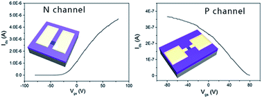
Herein, high-quality bulk InSe was grown by a low-cost pathway, after which mechanically exfoliated few-layer InSe nanosheets were obtained on a SiO2/Si substrate. The field-effect transistor (FET) devices with InSe channels were fabricated using two methods, including the shadow mask technique (SMT) and the ultraviolet lithography technique (ULT). Distinct different conducting characteristics were found in these devices on the basis of their manufacturing process, where the FET devices made by SMT displayed N-type channels, while P-type channels were obtained when ULT was used. Electrical and photoelectric properties studies demonstrated that the InSe devices made by SMT and ULT possess a high on/off ratio (4.7 × 10⁴ and 1.4 × 10²), mobility (18.7 cm2 V−1 s−1 and 0.33 cm2 V−1 s−1), photoresponsivity (0.59 A W−1 and 2.7 A W−1) and external quantum efficiency (115% and 527%), respectively. Theoretical and experimental investigation showed that the charge transfer between the H2O molecules and the InSe nanosheets caused the change in the conducting performances, and the defects led to an even heavier P-type doping effect in the channel.
 Please wait while we load your content...

