
Growth of single-crystalline cubic structured tin(ii) sulfide (SnS) nanowires by chemical vapor deposition†

Abstract
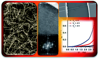
Single crystalline tin(II) sulfide (SnS) nanowires are synthesized using a chemical vapor deposition (CVD) method with the support of gold as catalyst. Field emission electron microscopy studies show that SnS nanostructures grown at temperatures between 600 and 700 °C have wire-like morphology. These nanowires have an average diameter between 12 and 15 nm with lengths up to several microns. These NWs consist of uniform and smooth surfaces, and exhibit nearly stoichiometric chemical composition (Sn/S = 1.13). Transmission electron microscopy analysis reveals that the NWs consist of single crystalline cubic crystal structure with a preferential growth direction of 〈100〉. Field-effect transistor devices fabricated with SnS nanowires show that the nanowires consist of p-type conductivity along with carrier density of 6 × 1018 cm−3.
 Please wait while we load your content...

