Transport properties of the top and bottom surfaces in monolayer MoS2 grown by chemical vapor deposition†
 *ab
*ab
Abstract
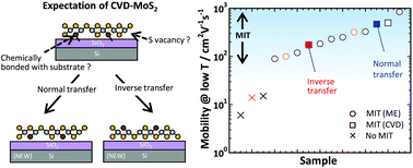
The advantage of MoS2, compared with graphene, is the direct growth on various oxide substrates by chemical vapor deposition (CVD) without utilizing catalytic metal substrates, which facilitates practical applications for electronics. The carrier mobility is, however, degraded from the intrinsic limit mainly due to short-range scattering caused by S vacancies formed during CVD growth. If the upper limit for the crystallinity of CVD-MoS2 on oxide substrates is determined by the MoS2/substrate interaction during growth, it will hinder the advantage. In this study, we investigated the interaction between monolayer MoS2 and a SiO2/Si substrate and the difference in crystallinity between the top and bottom S surfaces due to the MoS2/substrate interaction. Raman and photoluminescence spectroscopy indicated that doping and strain were induced in MoS2 from the substrate, but they could be removed by transferring MoS2 to a new substrate using polymers. The newly developed polymer-transfer technique enabled selective transfer of the bottom or top surface of CVD-MoS2 onto a new SiO2/Si substrate. The metal–insulator transition was clearly observed for both the normal and inverse transfers, suggesting that the crystallinity of CVD-MoS2 is high and that the crystallinity of the bottom surface interacting with the substrate was similar to that of the top free surface. These results provide positive prospects for the further improvement of the crystallinity of MoS2 on oxide substrates by reconsidering the growth conditions.
 Please wait while we load your content...

