Atomistic simulations of contact area and conductance at nanoscale interfaces
Abstract
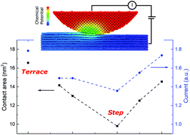
Atomistic simulations were used to study conductance across the interface between a nanoscale gold probe and a graphite surface with a step edge. Conductance on the graphite terrace was observed to increase with load and be approximately proportional to contact area calculated from the positions of atoms in the interface. The relationship between area and conductance was further explored by varying the position of the contact relative to the location of the graphite step edge. These simulations reproduced a previously-reported current dip at step edges measured experimentally and the trend was explained by changes in both contact area and the distribution of distances between atoms in the interface. The novel approach reported here provides a foundation for future studies of the fundamental relationships between conductance, load and surface topography at the atomic scale.


 Please wait while we load your content...