High performance transparent in-plane silicon nanowire Fin-TFTs via a robust nano-droplet-scanning crystallization dynamics†
Abstract
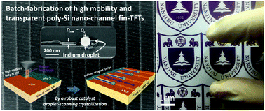
High mobility, scalable and even transparent thin-film transistors (TFTs) are always being pursued in the field of large area electronics. While excimer laser-beam-scanning can crystallize amorphous Si (a-Si) into high mobility poly-Si, it is limited to small areas. We here demonstrate a robust nano-droplet-scanning strategy that converts an a-Si:H thin film directly into periodic poly-Si nano-channels, with the aid of well-coordinated indium droplets. This enables the robust batch-fabrication of high performance Fin-TFTs with a high hole mobility of >100 cm2 V−1 s−1 and an excellent subthreshold swing of only 163 mV dec−1, via a low temperature <350 °C thin film process. More importantly, precise integration of tiny poly-Si channels, measuring only 60 nm in diameter and 2 μm apart on glass substrates, provides an unprecedented transparent Si-based TFT technology to visible light, which is widely sought for the next generation of high aperture displays and fully transparent electronics. The successful implementation of such a reliable nano-droplet-scanning strategy, rooted in the strength of nanoscale growth dynamics, will enable eventually the batch-manufacturing and upgrade of high performance large area electronics in general, and high definition and scalable flat-panel displays in particular.


 Please wait while we load your content...