Tuning the thickness of black phosphorus via ion bombardment-free plasma etching for device performance improvement†
Abstract
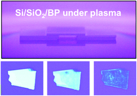
Layer-by-layer thinning without structural damage is essential for integrating two-dimensional materials (such as black phosphorus (BP)) in nanoelectronics, because their properties are primarily thickness-dependent. Unfortunately, most known etching processes for black phosphorus carry the possibility of structural degradation due to ion bombardment and thermal attack. In this study, we report a mild chemical thinning method free from causing physical damage, performed by modifying the sample configuration in a conventional reactive ion etching system. The thickness of mechanically exfoliated BP flakes can be easily controlled by modified plasma treatment, and these flakes maintain perfect crystallinity. Field-effect transistors based on thickness-controlled BP showed improved device performance after ion bombardment-free plasma etching. Our work provides a new way to realize the full potential of BP-based electronic devices.


 Please wait while we load your content...