Integration of p-type β-In2S3 thin films on III-nitride heterostructures for multiple functional applications†
Abstract
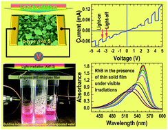
We report on the conversion of n-type InN thin films on top of III-nitride heterostructures to p-type β-In2S3 by post-growth heat treatments in a sulfur-vapor environment and address their photoelectrical and photocatalytic properties for functional integrations. Their electrical, structural, and spectroscopic evolutions as a function of sulfurization temperatures reveal an onset of surface passivation of InN at low temperatures (i.e., T < 550 °C) and the passivation is less effective at high temperatures. The conversion of InN to β-In2S3 starts at T ≥ 700 °C; the conversion increases with the sulfurization temperature and completes at T = 750 °C; and a further increase in the sulfurization temperature leads to a conversion of β-In2S3 to In2O3 due to the exhaustion of sulfur. The coherently strained InGaN buffer underneath the InN overlayer of the heterostructure is intact even at T = 800 °C. Photocurrent measurements do not show any apparent light responses for the thin films until sulfurized at T ≥ 700 °C while the photocatalytic degradation tests of rhodamine B (RhB) under visible irradiations (λ ≥ 400 nm) provide evidence for deethylation of RhB to DMRh (N,N-diehyl-N′-ethyl-rhodamine 110) on the surface of the thin films with higher activities on n-type InN and In2O3 than that on p-type β-In2S3 films. These observations, together with the intact InGaN underneath, open up a novel way to monolithic integrations of β-In2S3/InN based optical/photochemical sensors with GaN-based electronic devices (e.g., high-electron-mobility transistors) for advanced applications.


 Please wait while we load your content...