Self-organized growth of graphene nanomesh with increased gas sensitivity
Abstract
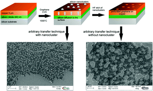
A bottom-up chemical vapor deposition (CVD) process for the growth of graphene nanomesh films is demonstrated. The process relies on silicon nanospheres to block nucleation sites for graphene CVD on copper substrates. These spheres are formed in a self-organized way through silicon diffusion through a 5 μm copper layer on a silicon wafer coated with 400 nm of silicon nitride. The temperature during the growth process disintegrates the Si3N4 layer and silicon atoms diffuse to the copper surface, where they form the nanospheres. After graphene nanomesh growth, the Si nanospheres can be removed by a simple hydrofluoric acid etch, leaving holes in the graphene film. The nanomesh films have been successfully transferred to different substrates, including gas sensor test structures, and verified and characterized by Auger, TEM and SEM measurements. Electrical/gas-exposure measurements show a 2-fold increase in ammonia sensitivity compared to plain graphene sensors. This improvement can be explained by a higher adsorption site density (edge sites). This new method for nanopatterned graphene is scalable, inexpensive and can be carried out in standard semiconductor industry equipment. Furthermore, the substrates are reusable.


 Please wait while we load your content...