Two-step fabrication of self-catalyzed Ga-based semiconductor nanowires on Si by molecular-beam epitaxy†
Abstract
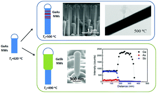
For the epitaxial growth of Ga-based III–V semiconductor nanowires (NWs) on Si, Ga droplets could provide a clean and compatible solution in contrast to the common Au catalyst. However, the use of Ga droplets is rather limited except for that in Ga-catalyzed GaAs NW studies in a relatively narrow growth temperature (Ts) window around 620 °C on Si. In this paper, we have investigated the two-step growth of Ga-catalyzed III–V NWs on Si (111) substrates by molecular-beam epitaxy. First, by optimizing the surface oxide, vertically aligned GaAs NWs with a high yield are obtained at Ts = 620 °C. Then a two-temperature procedure is adopted to preserve Ga droplets at lower Ts, which leads to an extension of Ts down to 500 °C for GaAs NWs. Based on this procedure, systematic morphological and structural studies for Ga-catalyzed GaAs NWs in the largest Ts range could be presented. Then within the same growth scheme, for the first time, we demonstrate Ga-catalyzed GaAs/GaSb heterostructure NWs. These GaSb NWs are axially grown on the GaAs NW sections and are pure zinc-blende single crystals. Compositional measurements confirm that the catalyst particles indeed mainly consist of Ga and GaSb sections are of high purity but with a minor composition of As. In the end, we present GaAsSb NW growth with a tunable Sb composition. Our results provide useful information for the controllable synthesis of multi-compositional Ga-catalyzed III–V semiconductor NWs on Si for heterogeneous integration.
 Please wait while we load your content...

