Nanoscale direct mapping of localized and induced noise sources on conducting polymer films†
Abstract
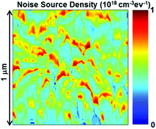
The localized noise-sources and those induced by external-stimuli were directly mapped by using a conducting-AFM integrated with a custom-designed noise measurement set-up. In this method, current and noise images of a poly(9,9-dioctylfluorene)-polymer-film on a conducting-substrate were recorded simultaneously, enabling the mapping of the resistivity and noise source density (NT). The polymer-films exhibited separate regions with high or low resistivities, which were attributed to the ordered or disordered phases, respectively. A larger number of noise-sources were observed in the disordered-phase-regions than in the ordered-phase regions, due to structural disordering. Increased bias-voltages on the disordered-phase-regions resulted in increased NT, which is explained by the structural deformation at high bias-voltages. On photo-illumination, the ordered-phase-regions exhibited a rather large increase in the conductivity and NT. Presumably, the illumination released carriers from deep-traps which should work as additional noise-sources. These results show that our methods provide valuable insights into noise-sources and, thus, can be powerful tools for basic research and practical applications of conducting polymer films.


 Please wait while we load your content...