Effect of the electric field during annealing of organic light emitting diodes for improving its on/off ratio†
Abstract
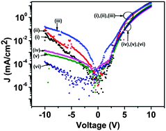
If an organic light emitting diode is to be used as part of a matrix addressed array, it should exhibit low reverse leakage current. In this paper we present a method to improve the on/off ratio of such a diode by simultaneous application of heat and electric field post device fabrication. A green OLED with excellent current efficiency was seen to be suffering from a poor on/off ratio of 102. After examining several combinations of annealing along with the application of a reverse bias voltage, the on/off ratio of the same device could be increased by three orders of magnitude, specifically when the device was annealed at 80 °C under reverse bias (−15 V) followed by slow cooling also under the same bias. Simultaneously, the forward characteristics of the device were relatively unaffected. The reverse leakage in the OLED is mainly due to the injection of minority carriers in the hole transport layer (HTL) and the electron transport layer (ETL), in this case, of holes in tris-(8-hydroxyquinoline)aluminum(Alq3) and electrons in 4,4′,4′′-tris(N-3-methylphenyl-N-phenylamino)triphenylamine (m-MTDATA). Hence, to investigate these layers adjacent to the electrodes, we fabricated their single layer devices. The possibility of bulk traps present adjacent to electrodes providing states for injection was ruled out after estimating the trap density both before and after the reverse biased annealing. The temperature independent current in reverse bias ruled out the possibility of thermionic injection. The origin of the reverse bias current is attributed to the availability of interfacial hole levels in Alq3 at the cathode work function level in the as-fabricated device; the suppression of the same being attributed to the fact that these levels in Alq3 are partly removed after annealing under an electric field.


 Please wait while we load your content...